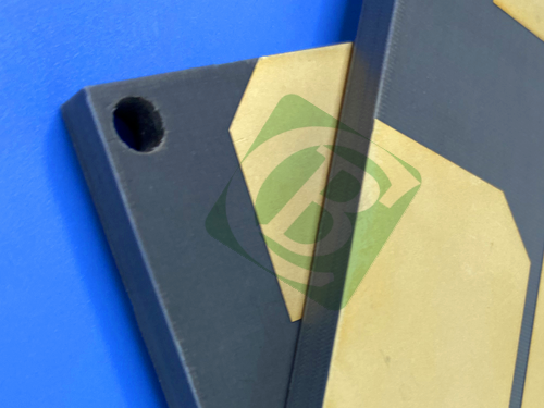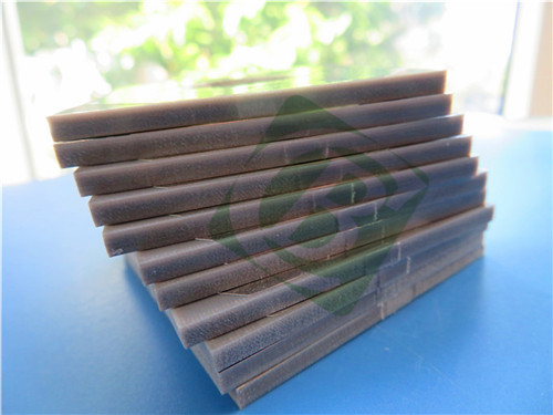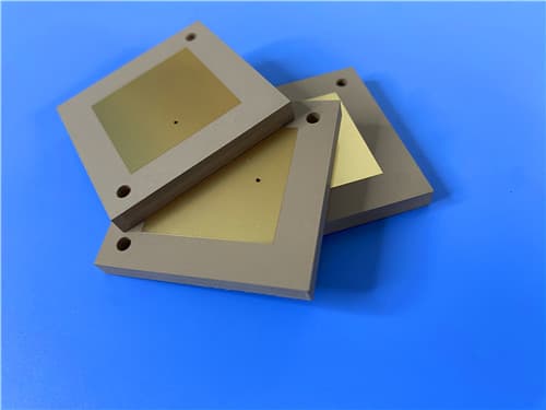
TP960 2-Layer 19.6mil High-Dk Thermoplastic PCB with ENIG Finish1.Introduction TP material is a unique high-frequency thermoplastic material in the industry. The dielectric layer of TP-type laminates consists of ceramics and polyphenylene Oxide resin (PPO), without fiberglass reinforcement. The dielectric constant can be precisely adjusted by adjusting the ratio between ceramics and PPO resin. The production process is special, and it has excellent dielectric performance and high reliability. TP refers to the smooth surface material without copper cladding, TP-1 refers to the material with copper cladding on one side, and TP-2 refers to the material with copper cladding on both sides. The dielectric constant can be arbitrarily selected within the range of 3 to 25 according to circuit requirements, and it is stable. Common dielectric constants include 3.0, 4.4, 6.0, 6.15, 9.2, 9.6, 9.8, 10.2, 11, 16, and 20. The dielectric loss is low, and the loss increases as the frequency increases, but the change is not significant within 10 GHz. The corresponding part numbers are TP300, TP440, TP600, TP615, TP920, TP960, TP980 etc. 2.Key Features Dielectric constant (Dk) of 9.6±0.19 at 10GHz 3.Benefits Unique ceramic-PPO thermoplastic composite without fiberglass reinforcement
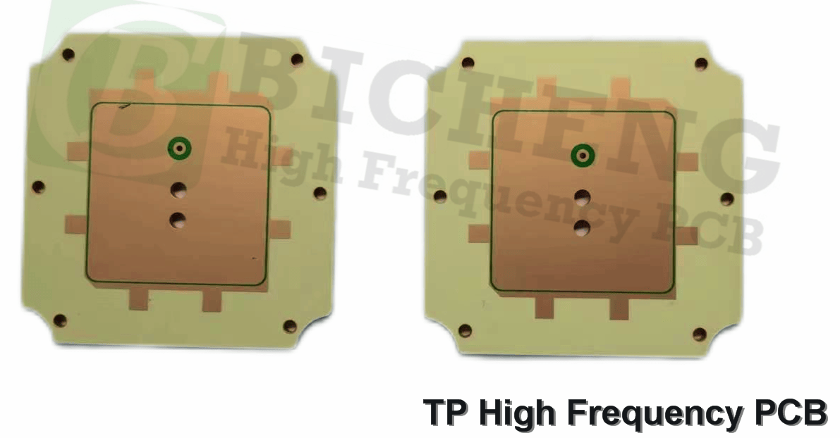
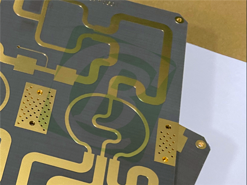
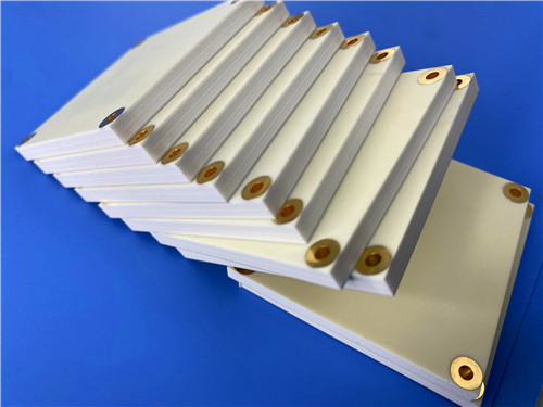
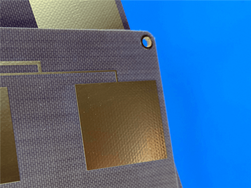
4.PCB Details
5.PCB Stackup (2-Layer Rigid Structure) Copper layer 1 – 35 μm 6.PCB Statistics Components: 56 7.Typical Applications Global Satellite Navigation System 8.Quality Assurance Artwork Format: Gerber RS-274-X |
Get a Quick Quote
Fill in the form below and our engineers will reply within 24 hours with technical specifications and pricing for TP960 2-Layer 19.6mil PCB.